Synthetic diamond is durable, inert, rigid, thermally conductive and chemically well-behaved—an elite material for both quantum and conventional electronics. But there’s one problem.
Diamond only likes diamond. It’s homoepitaxial, meaning it only grows on other diamonds, and integrating diamond into quantum or conventional computers, quantum sensors, cellphones, or other devices would mean sacrificing the diamond’s full potential or using large, expensive chunks of the precious material.
“Diamond stands alone in terms of its material properties, both for electronics—with its wide band gap, very best thermal conductivity, and exceptional dielectric strength—and for quantum technologies—it hosts nitrogen vacancy centers that are the gold standard for quantum sensing at room temperature,” said University of Chicago Pritzker School of Molecular Engineering Asst. Prof. Alex High. “But as a platform, it’s actually pretty terrible.”
A paper recently published in Nature Communications from the High Lab and Argonne National Laboratory has solved a major hurdle facing researchers working with diamond by creating a novel way of bonding diamonds directly to materials that integrate easily with either quantum or conventional electronics.
With this technique, the team directly bonded diamond with materials including silicon, fused silica, sapphire, thermal oxide, and lithium niobate without an intermediary substance to act as “glue.”
Perfect defects
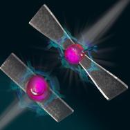
Unlike jewelers, quantum researchers prefer a slightly flawed diamond. By precisely engineering defects in the crystal lattice, researchers create durable qubits ideal for quantum computing, quantum sensing and other applications.
“Diamond is a wide bandgap material. It's inert. In effect, it's very well-behaved and has great thermal and electronic properties,” said paper co-author F. Joseph Heremans, who has a dual appointment with UChicago PME and Argonne. “Its raw physical properties tick a lot of marks that are beneficial to a lot of different fields. It was just very difficult to integrate with dissimilar materials until now.”
As thin diamond membranes were previously difficult to integrate directly into devices, this required larger (though still microscopic) chunks of the material. Paper co-author Avery Linder, a fourth-year undergraduate student, compared building sensitive quantum devices from these diamonds to trying to make a single grilled cheese sandwich with an entire block of cheddar.
To sidestep this problem, the scientists came up with a different approach.
“We make a surface treatment to the diamond and carrier substrates that makes them very attractive to each other. And by ensuring we have a pristine surface roughness, the two very flat surfaces will be bonded together,” said first author Xinghan Guo (Ph.D’24). “An annealing process enhances the bond and makes it really strong. That's why our diamond can survive various nanofabrication processes. It differentiates our process from simple placement of diamond on top of another material.”
In diamonds, each carbon atom shares electrons with four other carbon atoms. These electron-sharing bonds, called covalent bonds, create the gem’s hard, durable internal structure.
But if there is no other carbon atom nearby to share electrons, this creates what’s called “dangling bonds” on lonely atoms looking to partner. Creating a diamond surface full of these dangling bonds allowed the team to bond the nanometer-scale diamond wafers directly to other surfaces.
“You can almost think of it as like a sticky surface, because it wants to be attached to something else,” Linder said. “And so basically, what we've done is create sticky surfaces and put them together.”
Instead of the several-hundred-microns-thick bulk diamonds typically used to study quantum qubits, the team bonded crystalline membranes as thin as 100 nanometers while still maintaining suitability for advanced quantum applications.
Overcoming challenges
UChicago PME Asst. Prof. Peter Maurer, a co-author on the paper, works in quantum bio-sensing, using revolutionary quantum techniques to obtain better, more accurate measurements of the working of fundamental biological processes at the micro- and nanoscale.
“Although we have overcome many challenges associated with interfacing intact biological targets with diamond-based quantum sensors, their integration into actual measurements devices, such as a commercial microscope or a diagnostic device, while not losing readout efficiency, has remained an outstanding challenge,” Maurer said. “This new work with diamond membranes bonding that Alex’s lab led has gotten around many of these issues and brings us an important step closer to applications.”
“This new technique has the potential to greatly influence the ways we do quantum and even phone or computer manufacturing,” Linder said.
The researchers have patented the process and are commercializing it through the University of Chicago’s Polsky Center for Entrepreneurship and Innovation.
High compares the new diamond technique to the advances in complementary metal-oxide semiconductors (CMOS) over the years, from bulky individual transistors in labs in the 1940s to the powerful, tiny integrated circuits filling computers and phones today.
“We’re hoping that our ability to generate these thin films and integrate them in a scalable fashion can lead to something like CMOS-style revolution for diamond-based quantum technologies,” he said.
Citation: “Direct-bonded diamond membranes for heterogeneous quantum and electronic technologies,” Guo et al, Nature Communications, October 10, 2024.
Funding: U.S. Department of Energy Office of Science Q-NEXT center, National Science Foundation
Adapted from an article first published by the Pritzker School of Molecular Engineering.