Let’s say you’re an engineer with an idea for a new car. But before you even can start experimenting, you have to spend hours casting screws and making rubber for tires from scratch.
This is similar to the challenge facing researchers trying to invent new kinds of technology. The ability to make, say, a flexible screen or a new solar panel, starts with discovering a new combination of materials with unusual properties at the atomic scale. But in the field of 2D materials, which is considered one of the most exciting areas for future electronics, scientists still have to laboriously hand-make each new potential material before they can test its capabilities.
A new technique asks a robot to lend a hand. Developed by scientists from the University of Chicago, Cornell University and the University of Michigan, the research lays out an innovative manufacturing method for assembling nanomaterials.
The scientists hope the process, published Jan. 24 in Nature Nanotechnology, could speed the pace of breakthroughs in the field.
“This process is fully automated—you can program it and walk away,” said co-first author Andrew Mannix, a former University of Chicago Kadanoff-Rice postdoctoral fellow who is now an assistant professor at Stanford University. “Previously, if you wanted to try 10 different permutations of materials, it would all be done by hand, which is weeks of labor. We can now do this in an hour. We hope this opens new lines of inquiry in this exciting field by reducing the tediousness of labor.”
A tiny assembly line
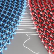
The field of 2D materials involves stacking sheets that are each only a few atoms thick. When the layers are this thin, even ordinary materials often produce surprising new behaviors. For example, carbon suddenly displays superconductivity, the ability to conduct electricity flawlessly, when two layers are vertically stacked at a “magic” angle.
Scientists are especially interested in stacking together different kinds of 2D materials, Mannix said: “It’s been realized recently that if you can take these layers and stack them with control over the crystal orientation, you can get some really beautiful new physics, because the interactions between the layers are modified.”
However, the discovery process is limited and slow, because scientists must first painstakingly assemble these combinations and test them one by one.
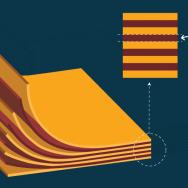
UChicago scientists set out to address this problem. Led by Prof. Jiwoong Park, an expert on nanomaterials, the group had already invented a way to make intricate atomically-thin sheets and to peel them up and stack them together. Now they needed a way to automate this process.
They wanted to make a sort of tiny assembly line, but each component of the manufacturing process came with its own challenges. First, the scientists had to figure out a way to precisely cut their sheets into the exact shapes they wanted, which is difficult to do cleanly without breaking or damaging the sheets. “With experimentation, we found a technique that could achieve large-area patterning, with very high precision and without contaminating the material,” said Andrew Ye, a Ph.D. student in Park’s lab and the other co-first author of the paper.
The next challenge was making a robot “hand” capable of maneuvering these extremely fragile sheets. “I needed to find a polymer that was precise enough to pick up the sheets,” said Mannix, “but also capable of letting it down again—gently and in the exact right spot.”
They came up with a “hand” made of soft polymers that fall apart when exposed to heat or ultraviolet light. Once the sheet is precisely positioned, the hand dissolves and the sheet drops into place.
With this system, the scientists could now program their assembly line to make a material structure with dozens of different layers, walk away, and come back to a finished sample ready to test in a matter of minutes.
Not only is the system very precise, but it also offers extensive options for customization, including the coveted ability to rotate each successive sheet at different angles.
“When we started looking at this problem, it seemed unimaginable to automate it,” said Park, who is appointed in both the Department of Chemistry and the Pritzker School of Molecular Engineering. “This should speed up the pace of discovery considerably. It’s kind of like the difference between handwriting a book letter by letter versus using a printing press.”
The other authors on the study included University of Chicago graduate students Fauzia Mujid and Robert Shreiner; postdoctoral researchers Myungjae Lee and Jong-Hoon Kang; Chibeom Park, formerly a postdoctoral researcher and now at the Samsung Electronics Semiconductor Research Center; Prof. Alex High of the Pritzker School of Molecular Engineering and Argonne National Laboratory; Ariana Ray and Prof. David Muller of Cornell; and Suk Hyun Sung and Prof. Robert Hovden of the University of Michigan.
The research made use of the University Chicago Materials Research Science and Engineering Center, the Pritzker Nanofabrication Facility, the Searle Cleanroom, the Michigan Center for Materials Characterization, and the Cornell Center for Materials Research.
Citation: “Robotic Four-Dimensional Pixel Assembly of van der Waals Solids.” Mannix et al, Nature Nanotechnology, Jan. 24, 2022.
Funding: National Science Foundation, Air Force Office of Scientific Research, Samsung Advanced Institute of Technology, Department of Defense, W.M. Keck Foundation, Army Research Office.