Moving heat around where you want it to go—adding it to houses and hairdryers, removing it from car engines and refrigerators—is one of the great challenges of engineering.
All activity generates heat, because energy escapes from everything we do. But too much can wear out batteries and electronic components—like parts in an aging laptop that runs too hot to actually sit on your lap. If you can’t get rid of heat, you’ve got a problem.
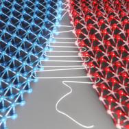
Scientists at the University of Chicago have invented a new way to funnel heat around at the microscopic level: a thermal insulator made using an innovative technique. They stack ultra-thin layers of crystalline sheets on top of each other, but rotate each layer slightly, creating a material with atoms that are aligned in one direction but not in the other.
“Think of a partly-finished Rubik’s cube, with layers all rotated in random directions,” said Shi En Kim, a graduate student with the Pritzker School of Molecular Engineering who is the first author of the study. “What that means is that within each layer of the crystal, we still have an ordered lattice of atoms, but if you move to the neighboring layer, you have no idea where the next atoms will be relative to the previous layer—the atoms are completely messy along this direction.”
The result is a material that is extremely good at both containing heat and moving it, albeit in different directions—an unusual ability at the microscale, and one that could have very useful applications in electronics and other technology.
“The combination of excellent heat conductivity in one direction and excellent insulation in the other direction does not exist at all in nature,” said study lead author Jiwoong Park, professor of chemistry and molecular engineering at the University of Chicago. “We hope this could open up an entirely new direction for making novel materials.”
‘Just amazingly low’
Scientists are constantly on the search for materials with unusual properties, because they can unlock completely new capabilities for devices such as electronics, sensors, medical technology or solar cells. For example, MRI machines were made possible by the discovery of a strange material that can perfectly conduct electricity.
Park’s group had been investigating ways to make extremely thin layers of materials, which are just a few atoms thick. Normally, the materials used for devices are made up of extremely regular, repeating lattices of atoms, which makes it very easy for electricity (and heat) to move through the material. But the scientists wondered what would happen if they instead rotated each successive layer slightly as they stacked them.
They measured the results and found that a microscopic wall made of this material was extremely good at preventing heat from moving between compartments. “The thermal conductivity is just amazingly low—as low as air, which is still one of the best insulators we know,” said Park. “That in itself is surprising, because it’s very unusual to find that property in a material that is a dense solid—those tend to be good heat conductors.”
But the point that was really exciting for the scientists was when they measured the material’s ability to transport heat along the wall, and found it could do so very easily.
Those two properties in combination could be very useful. For example, making computer chips smaller and smaller results in more and more power running through a small space, creating an environment with a high “power density”—a dangerous hotspot, said Kim.
“You’re basically baking your electronic devices at power levels as if you are putting them in a microwave oven,” she said. “One of the biggest challenges in electronics is to take care of heat at that scale, because some components of electronics are very unstable at high temperatures.
“But if we can use a material that can both conduct heat and insulate heat at the same time in different directions, we can siphon heat away from the heat source—such as the battery—while avoiding the more fragile parts of the device.”
That capability could open doors to experiment with materials that have been too heat-sensitive for engineers to use in electronics. In addition, creating an extreme thermal gradient—where something is very hot on one side and cool on the other—is difficult to do, particularly at such small scales, but could have many applications in technology.
“If you think of what the windowpane did for us—being able to keep the outside and inside temperatures separate—you can get a sense of how useful this could be,” Park said.
The scientists only tested their layering technique in one material, called molybdenum disulfide, but think this mechanism should be general across many others. “I hope this opens up a whole new direction for making exotic thermal conductors,” Kim said.
The research used the University of Chicago Materials Research Science and Engineering Center and the Pritzker Nanofabrication Facility.
Other coauthors were UChicago graduate students Fauzia Mujid and Preeti Poddar; postdoctoral fellows Chibeom Park (now at Samsung Electronics Semiconductor Research Center), Joonki Suh (now at UNIST) and Yu Zhong; as well as David Cahill and Akash Rai with the University of Illinois at Urbana-Champaign, Paul Erhart, Fredrik Eriksson, and Erik Fransson with the Chalmers University of Technology in Sweden, and David Muller and Ariana Ray with Cornell University.
Citation: “Extremely anisotropic van der Waals thermal conductors.” Kim et al, Nature, Sept. 29, 2021.
Funding: U.S. Air Force Office of Scientific Research, National Science Foundation, Samsung Advanced Institute of Technology, Camille and Henry Dreyfus Foundation.

