Spinning information
The work follows on a previous study in which the researchers observed changes in the spin state of the defect’s electrons when the material was similarly strained. Because these defects are well isolated within the crystal, they can act as “carriers” of information. When the electrons trapped near the defects change between spin states, they emit energy in the form of photons. Depending on which state the electrons are in, they emit either more or fewer photons in a technique known as spin-dependent readout.
In the experiment, the researchers sought to assess the relationship between the sound energy used to produce the strain on the defects in the crystal lattice and the spin transitions indicated by the emitted photons. While the defects in the crystal naturally fluoresce, the additional strain causes the ground spin of the electron to change state, resulting in a coherent manipulation of the spin state than can be measured optically.
“We wanted to see the coupling between the sound strain and the light response, but to see exactly what the coupling between them is, you need to know both how much strain you’re applying, and how much more optical response you’re getting out,” said Holt.
The electrodes used to generate the sound waves are roughly five microns in width—far larger than the defects themselves, which consist of two missing atoms known as a divacancy complex. The sound wave strains the defects by alternately pushing and pulling on them, causing the electrons to change their spins.
Taking a closer look
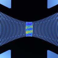
To characterize the lattice and defects, the researchers used a unique facility located at Argonne: the Hard X-ray Nanoprobe beamline, operated jointly at the laboratory’s Center for Nanoscale Materials and Advanced Photon Source. Through a newly developed technique called stroboscopic Bragg diffraction microscopy, Holt and his colleagues were able to image the lattice around the defects at many different points throughout the strain cycle.
“We’re interested in how to manipulate the original spin state with acoustic waves, and how you can spatially map out the mechanics of the strain with X-rays,” said PME and Argonne materials scientist Joseph Heremans, another author of the study.
“The X-rays measure exactly the lattice distortion,” Holt added.
Stroboscopic Bragg diffraction involves synchronizing the frequency of the acoustic wave to the frequency of the electron pulses in the Advanced Photon Source’s storage ring. In this way, the researchers were essentially able to “freeze the wave in time,” according to Holt. This allowed them to create a series of images of the strain experienced by the lattice at each point on the wave.
“It’s like if you had ripples in a pond, and you could shine a light on one spot of the pond,” Holt said. “You’d see a movement of peak to trough, and trough to peak.”
“We’re directly imaging sound’s footprint going through this crystal,” Heremans added. “The sound waves cause the lattice to curve, and we can measure exactly how much the lattice curves by going through a specific point of the lattice at a specific point in time.”
Additional collaborators included University of Chicago graduate student Samuel Whiteley and UChicago and Argonne Gary Wolfowicz.
Citation: “Correlating dynamic strain and photoluminescence of solid-state defects with stroboscopic X-ray diffraction microscopy.” Whiteley et al, Nature Communications, July 29, 2019. https://www.nature.com/articles/s41467-019-11365-9
Funding: U.S. Department of Energy, Air Force Office of Scientific Research.
—Story first appeared on the Argonne National Laboratory website.


 —Prof. Chuan He